CMNT3904E NPN
CMNT3906E PNP
ENHANCED SPECIFICATION
SURFACE MOUNT
COMPLEMENTARY
SILICON TRANSISTOR
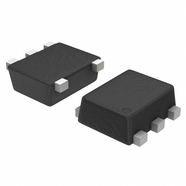
SOT-953 CASE
w w w. c e n t r a l s e m i . c o m
DESCRIPTION:
The CENTRAL SEMICONDUCTOR CMNT3904E
and CMNT3906E Low VCE(SAT) NPN and PNP
Transistors, respectively, are designed for applications
where ultra small size and power dissipation are
the prime requirements. Packaged in an SOT-953
package, these components provide performance
characteristics suitable for the most demanding size
constrained applications.
MARKING CODES: CMNT3904E: CL
CMNT3906E: CM
FEATURES
APPLICATIONS
•
•
•
•
•
•
•
•
Very Small Package Size
Low Package Profile, 0.5mm
200mA Collector Current
Low VCE(SAT) (0.1V Typ @ 50mA)
• Small, 1 x 0.8mm, SOT-953
Surface Mount Package
MAXIMUM RATINGS: (TA=25°C)
♦ Collector-Base Voltage
Collector-Emitter Voltage
♦ Emitter-Base Voltage
Continuous Collector Current
Power Dissipation
Operating and Storage Junction Temperature
Thermal Resistance
DC-DC Converters
Voltage Clamping
Protection Circuits
Battery powered equipment including:
Cell Phones, Digital Cameras, Pagers,
PDAs, Laptop Computers, etc.
SYMBOL
UNITS
VCBO
VCEO
60
40
V
VEBO
IC
6.0
V
200
mA
PD
TJ, Tstg
250
-65 to +150
mW
°C
ΘJA
500
°C/W
ELECTRICAL CHARACTERISTICS: (TA=25°C unless otherwise noted)
NPN
SYMBOL
TEST CONDITIONS
MIN
TYP
ICEV
VCE=30V, VEB=3.0V
♦ BVCBO
IC=10µA
60
115
BVCEO
IC=1.0mA
40
60
♦ BVEBO
IE=10µA
6.0
7.5
♦ VCE(SAT)
IC=10mA, IB=1.0mA
.057
♦ VCE(SAT)
IC=50mA, IB=5.0mA
0.1
VBE(SAT)
IC=10mA, IB=1.0mA
0.65
0.75
VBE(SAT)
♦ hFE
♦ hFE
IC=50mA, IB=5.0mA
VCE=1.0V, IC=0.1mA
VCE=1.0V, IC=1.0mA
90
100
0.85
240
235
PNP
TYP
90
55
7.9
.05
0.1
0.75
0.85
130
150
V
MAX
50
0.1
0.2
UNITS
nA
V
V
V
V
V
0.85
0.95
V
V
♦ Enhanced Specification
R3 (16-March 2020)
�CMNT3904E NPN
CMNT3906E PNP
ENHANCED SPECIFICATION
SURFACE MOUNT
COMPLEMENTARY
SILICON TRANSISTOR
ELECTRICAL CHARACTERISTICS - Continued:
SYMBOL TEST CONDITIONS
MIN
hFE
VCE=1.0V, IC=10mA
100
♦ hFE
VCE=1.0V, IC=50mA
70
hFE
VCE=1.0V, IC=100mA
30
fT
VCE=20V, IC=10mA, f=100MHz
300
Cob
VCB=5.0V, IE=0, f=1.0MHz
Cib
VBE=0.5V, IC=0, f=1.0MHz
hie
VCE=10V, IC=1.0mA, f=1.0kHz
1.0
hre
VCE=10V, IC=1.0mA, f=1.0kHz
0.1
hfe
VCE=10V, IC=1.0mA, f=1.0kHz
100
hoe
VCE=10V, IC=1.0mA, f=1.0kHz
1.0
NF
VCE=5.0V, IC=100μA, RS =1.0kΩ,
f=10Hz to 15.7kHz
td
VCC=3.0V, VBE=0.5V, IC=10mA, IB1=1.0mA
tr
VCC=3.0V, VBE=0.5V, IC=10mA, IB1=1.0mA
ts
VCC=3.0V, IC=10mA, IB1=IB2=1.0mA
tf
VCC=3.0V, IC=10mA, IB1=IB2=1.0mA
NPN
TYP
215
110
50
PNP
TYP
150
120
55
MAX
300
4.0
12
12
10
400
60
4.0
35
35
200
50
UNITS
MHz
pF
pF
kΩ
X10-4
μS
dB
ns
ns
ns
ns
♦ Enhanced Specification
SOT-953 CASE - MECHANICAL OUTLINE
LEAD CODE:
1) Collector
2) Collector
3) Collector
4) Emitter
5) Base
CMNT3904E
MARKING CODE: CL
CMNT3906E
MARKING CODE: CM
R3 (16-March 2020)
w w w. c e n t r a l s e m i . c o m
�OUTSTANDING SUPPORT AND SUPERIOR SERVICES
PRODUCT SUPPORT
Central’s operations team provides the highest level of support to insure product is delivered on-time.
• Supply management (Customer portals)
• Custom bar coding for shipments
• Inventory bonding
• Custom product packing
• Consolidated shipping options
DESIGNER SUPPORT/SERVICES
Central’s applications engineering team is ready to discuss your design challenges. Just ask.
• Free quick ship samples (2nd day air)
• Special wafer diffusions
• Online technical data and parametric search
• PbSn plating options
• SPICE models
• Package details
• Custom electrical curves
• Application notes
• Environmental regulation compliance
• Application and design sample kits
• Customer specific screening
• Custom product and package development
• Up-screening capabilities
REQUESTING PRODUCT PLATING
1. If requesting Tin/Lead plated devices, add the suffix “ TIN/LEAD” to the part number when
ordering (example: 2N2222A TIN/LEAD).
2. If requesting Lead (Pb) Free plated devices, add the suffix “ PBFREE” to the part number
when ordering (example: 2N2222A PBFREE).
CONTACT US
Corporate Headquarters & Customer Support Team
Central Semiconductor Corp.
145 Adams Avenue
Hauppauge, NY 11788 USA
Main Tel: (631) 435-1110
Main Fax: (631) 435-1824
Support Team Fax: (631) 435-3388
www.centralsemi.com
Worldwide Field Representatives:
www.centralsemi.com/wwreps
Worldwide Distributors:
www.centralsemi.com/wwdistributors
For the latest version of Central Semiconductor’s LIMITATIONS AND DAMAGES DISCLAIMER,
which is part of Central’s Standard Terms and Conditions of sale, visit: www.centralsemi.com/terms
w w w. c e n t r a l s e m i . c o m
(001)
�


 工商网监
湘ICP备2023018690号
工商网监
湘ICP备2023018690号